EMC/EMI Compliance in PCB Design
Electromagnetic Compatibility (EMC) means that an electronic device both manages its own electromagnetic emissions and withstands interference from external sources. Every product seeking CE or FCC certification must pass EMC tests. EMC rules ignored at the design stage can translate into thousands of dollars in revision costs at the test lab.
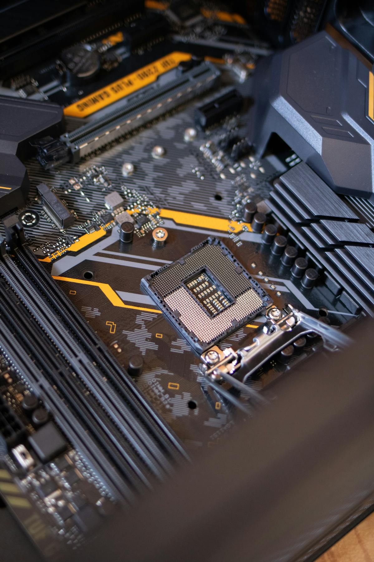
Sources of EMC Problems
- High-speed signals: SPI, I²C, USB, Ethernet traces can act like powerful antennas.
- Power conversion circuits: DC-DC converters generate switching noise.
- Ground plane splits: Inadequate or split GND planes cause common impedance issues.
- Via transitions: High-frequency signals experience impedance discontinuity when changing layers.
EMC Strategies in PCB Layout
1. Stackup Planning
In PCBs with 4 or more layers, sandwiching signal layers between GND/PWR plane layers dramatically reduces EMI emissions. A minimum 4-layer stackup is recommended: SIG | GND | PWR | SIG.
2. Continuous Ground Plane
Never split the GND plane. Split ground planes create current loops and consequently high emissions. If you want physical separation between analog and digital circuits, achieve it through layout — not plane splitting.
3. Decoupling Capacitors
Place 100nF + 10µF decoupling capacitors as close as possible to each IC's power pin. Keep vias as short as possible; don't place other components between the capacitor and the pin.
4. High-Speed Trace Routing
Route differential pairs (USB, Ethernet, LVDS) with balanced length and in close proximity. Avoid 90° corners; use 45° or arc corners. Keep trace lengths as short as possible.
Filter and Protection Components
Add ferrite beads and common-mode chokes to I/O lines. Apply LC filters to noisy power lines. Use TVS diodes or varistors for ESD protection — especially on external connectors, USB, and I/O pins.
"Planning EMC at the schematic stage — not as an afterthought — both shortens and reduces the cost of the certification process."
— MECRONIC Electronic Design Team
At MECRONIC, every PCB design begins with EMC pre-analysis and stackup planning. We target a prototype that is certification-ready — minimizing redesign cycles.